Excess 3 Adder Circuit Diagram Explain Full Adder With Truth
Full adder circuit – how it works Excess 3 to bcd conversion Adder excess
Design A Full Adder And Subtractor Circuit
Figure 1 from analysis and design of reversible excess-3 adder and Solved design an excess-3 adder circuit that adds two valid 3 bit full adder
Design a full adder and subtractor circuit
Design a full adder and subtractor circuitAnalysis and design of reversible excess-3 adder and subtractor Digital logic design full adder circuitExcess 3 adder circuit diagram.
Solved design an excess- 3 adder circuit that adds two validBinary adder circuit diagram Excess 3 adderExcess 3 adder || excess 3 addition || digital logic design || digital.
4 bit adder subtractor truth table
4 bit adder circuit diagramAdder excess reversible subtractor Excess 3 to bcd circuit diagramExcess 3 adder circuit diagram.
[diagram] 8 bit adder circuit diagramHow to build a full adder circuit Full adder circuit diagram on breadboardHow to build a full adder circuit.

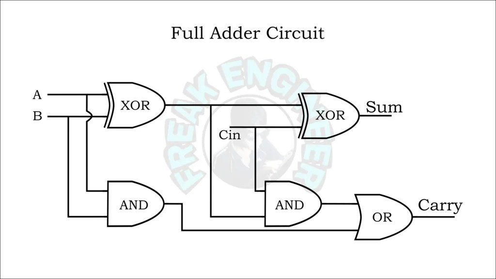
Explain full adder with truth table and logic circuit diagram
4 bit binary adder circuit diagramFull adder Cd4008 4-bit full adder ic pinout, working, example and datasheetBlock diagram of basic full adder circuit.
Excess-3 adderAdder bit full spice youspice electronics digital projects [diagram] bcd to excess 3 logic diagramBcd to excess 3 code conversion » freak engineer.

Adder bits logic sumador binario datasheet inputs suma pinout microcontrollerslab
.
.

![[DIAGRAM] Bcd To Excess 3 Logic Diagram - MYDIAGRAM.ONLINE](https://i2.wp.com/www.deldsim.com/circuit_diagram/39.png)
[DIAGRAM] Bcd To Excess 3 Logic Diagram - MYDIAGRAM.ONLINE

Excess 3 Adder Circuit Diagram
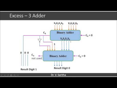
Excess 3 Adder - YouTube

CD4008 4-Bit Full ADDER IC pinout, working, example and datasheet

Block Diagram of basic full adder circuit | Download Scientific Diagram
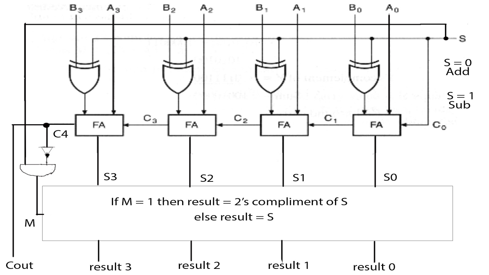
Design A Full Adder And Subtractor Circuit

Figure 1 from Analysis and design of reversible excess-3 adder and

Solved Design an Excess- 3 adder circuit that adds two valid | Chegg.com